

D10-Core_Cascade: Custom 8-Core SIMT GPGPU
Abstract
Abstract
Aim
The primary objective of this project is to demystify the fundamental architecture of modern hardware accelerators by designing, simulating, and physically implementing a custom Single Instruction, Multiple Threads (SIMT) Graphics Processing Unit (GPU) from scratch. By building a fully functional General-Purpose GPU (GPGPU) and deploying it as a physical System-on-Chip (SoC) on a Nexys 4 DDR board, we aim to expose the underlying mechanics of thread dispatching, memory arbitration, parallel execution, and physical silicon tape-out readiness.
Introduction
While modern commercial GPUs have grown into immensely complex, proprietary black boxes, this project takes a first-principles approach to hardware design. Operating on the SIMT execution model, our architecture groups threads into blocks that execute the exact same instruction synchronously across multiple data streams, enabling massive parallelization. Expanding upon a 2-core foundation, our final architecture features an 8-core compute cluster capable of managing 32 parallel threads in flight synchronously. To guarantee timing closure and prevent metastable states, the compute domain steps safely at a tuned 95 MHz clock speed. To interface this mathematical processing engine with the physical world, the system includes an asynchronous dual-clock VGA pipeline driving an 800x600 resolution display, paired with a Memory-Mapped I/O (MMIO) navigation controller for real-time hardware interaction.
Literature Survey and Technologies Used
Literature & Architecture Survey:
- SIMT vs. Sequential Execution: Unlike traditional CPUs that rely on out-of-order execution, SIMT architectures minimize the overhead of fetching and decoding instructions by sharing a single program counter across multiple threads.
- Open-Source GPU Foundations: This work builds upon the foundational concepts of the open-source "Tiny-GPU" project by Adam Majmudar, vastly expanding its capabilities from a 2-core 16-bit proof-of-concept into a 32-bit, high-resolution 8-core SoC.
Technologies & Tools Used:
- Hardware Description: SystemVerilog for RTL design and simulation.
- Synthesis & FPGA: Xilinx Vivado Design Suite, deployed on the Digilent Nexys 4 DDR board (Artix-7 XC7A100T).
- ASIC Flow: OpenLane EDA toolchain targeting the open-source Skywater 130nm process node.
Methodology
1. GPU Architecture and SIMT Execution
1.1 System Integration & Multi-Core Scaling
The core of the GPU acts as a massive parallel execution engine driven by a 32-bit Device Control Register (DCR). The system was scaled from a minimal 2-core foundation to a highly robust 8-core compute cluster capable of managing 32 parallel threads in flight synchronously. A central hardware Dispatcher breaks down the total workload (e.g., 480,000 threads for an 800x600 display) into blocks of 4 threads. During initial scaling, a severe stalling failure was discovered where the single-cycle start pulse deactivated the dispatcher prematurely. This was resolved by redesigning the dispatcher’s state machine to include a dedicated active state register, ensuring it continuously routes blocks to idle cores until the total thread count is reached.
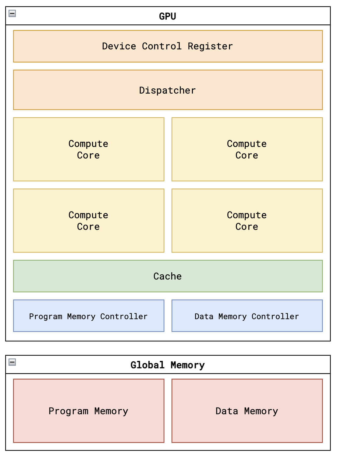
Figure 1: Top-level block diagram integrating the GPU Cores, Dispatcher, DCR, and Memory.
1.2 Core Execution Pipeline
Each compute core operates independently using an active-state finite state machine (FSM). The pipeline is divided into seven distinct stages to guarantee memory latencies do not corrupt arithmetic execution: FETCH, DECODE, REQUEST, WAIT, EXECUTE, UPDATE, and DONE. Because Vivado assumes worst-case Process, Voltage, and Temperature (PVT) conditions during Static Timing Analysis (STA), clocking wizards (clk_wiz IP) were used to safely step the compute domain down to 95 MHz, thereby sealing off timing violations and guaranteeing physical safety across the die.
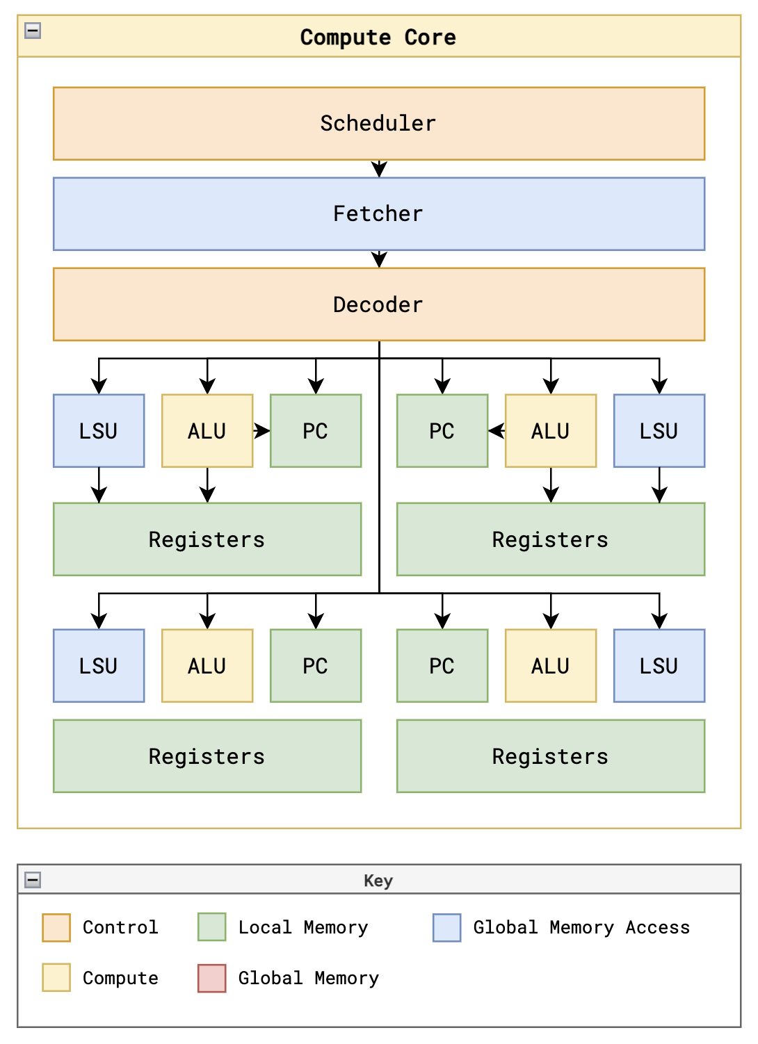
Figure 2: Datapath of a single Compute Core, highlighting the Fetcher, Decoder, ALU, LSU, PC, and the 4 independent Thread Register Files.
2. Custom Instruction Set Architecture & Arithmetic
2.1 ISA Expansion and Intentional Features
The GPU executes a custom 16-bit Instruction Set Architecture (ISA). To support advanced matrix operations, new instructions were added, including FIXED_MUL, SLL, SRL, SRA, and LUI. During the design of the custom decoder, two intentional architectural features were formalized: Absolute Branching (routing the immediate value directly to the PC to simplify assembly jump logic) and Immediate Sign-Extension (leveraging the MSB to pad 8-bit immediates into 32-bit inputs so 2's complement arithmetic remains perfectly intact).
2.2 Q8.24 Fixed-Point Arithmetic & DSP Optimization
To compute the Mandelbrot set accurately, the arithmetic logic was upgraded to a 32-bit Q8.24 fixed-point number system. A brilliant algorithmic hardware pivot was made to avoid the massive routing delays of hardware division (DIV). Division was optimized natively in software by storing reciprocal values inside the configuration memory (e.g., 32'h000051EC for 1/800). The GPU then utilized the FIXED_MUL instruction to perform division by reciprocal multiplication. This massive architectural shift consumed exactly 1 extra DSP slice while successfully bypassing severe timing violations.
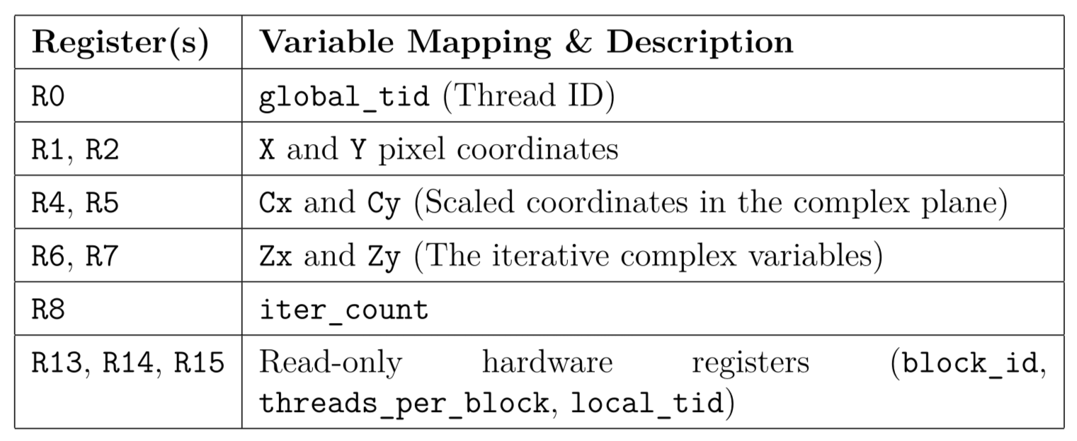
Figure 3: Register Map Cheat Sheet utilized for the Mandelbrot kernel, detailing the assignment of general-purpose calculation registers and hardwired SIMT thread indices.
3. Algorithmic Mapping: The Mandelbrot Kernel
The Mandelbrot set is an escape-time fractal calculated over the complex plane using the iterative formula Zn+1 = Zn2 + C. Because the GPU's CONST instruction is constrained to 8-bit immediate values, the 32-bit fixed-point configuration parameters (coordinate boundaries, step sizes, and the reciprocal for division) were pre-calculated by the host and loaded into the initial addresses of the Data Memory. By executing a highly optimized custom assembly kernel, adjacent threads process neighboring pixels, creating massive SIMT parallelization.
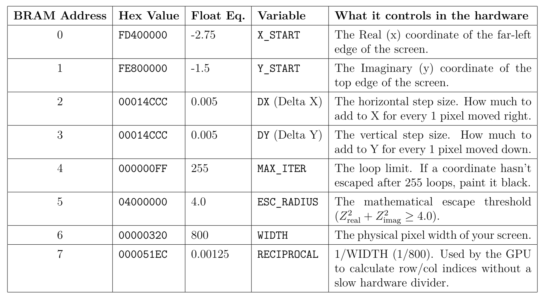
Figure 4: Data Memory mapping for the Mandelbrot kernel. The 32-bit Q8.24 fixed-point constants are stored in the first 8 memory addresses to be loaded into registers via LDR instructions.
4. Memory Architecture & Asynchronous VGA Pipeline
4.1 Dual-Clock Domain Crossing
Interfacing a high-speed parallel GPU with a sequential display controller introduces a critical clock-domain mismatch. Driving an 800x600 resolution requires a strict 40 MHz display clock, while the GPU computes at 95 MHz. To safely cross these domains, a top-level wrapper instantiates an asynchronous Dual-Port BRAM Framebuffer. The 8-core GPU continuously writes computed pixel data asynchronously to Port A, while the VGA controller sequentially reads from Port B to draw the screen, avoiding metastable crashes and visual tearing.
4.2 Hardware Color Mapper & Memory Optimization
Rendering an 800x600 display requires storing 480,000 discrete pixels. If the GPU calculated and stored full 24-bit RGB colors, it would consume massive amounts of block RAM and suffocate the internal memory buses. Instead, the GPU solely calculates the escape-time iteration count and stores it as an 8-bit integer in the Framebuffer. A combinational hardware decoder, the color_mapper.sv, interprets this 8-bit count on the fly and translates it into a 12-bit VGA color signal using a high-diversity, polychromatic gradient Look-Up Table (LUT).
4.3 Memory-Mapped I/O (MMIO) & Hardware Navigation
Real-time user interaction with the fractal was achieved without needing to interrupt the GPU. A hardware debouncer conditions the physical button presses on the Nexys 4 board, which a navigation controller uses to dynamically overwrite the global coordinate constants (X_MIN, Y_MIN) stored in the configuration memory. On the very next frame, the GPU seamlessly loads the updated coordinates via MMIO and begins computing the new panned or zoomed view.
5. ASIC Design Flow: RTL-to-GDSII
To prove that the custom GPU architecture is not only suitable for FPGA emulation but is completely tape-out ready for physical silicon manufacturing, a full Application-Specific Integrated Circuit (ASIC) design flow was executed. Targeting the base 2-core configuration, the SystemVerilog RTL was passed through the open-source OpenLane EDA toolchain utilizing the Skywater 130nm process node.
5.1 Clock Tree Synthesis (CTS) & Layout Generation
The physical design process was driven by a custom TCL script, configured for relative sizing with a target core utilization of 35% and an area optimization strategy (AREA 0). To prevent severe hold-time violations and data corruption during thread synchronization, the toolchain synthesized a balanced, hierarchical clock distribution network (CTS) targeting a strict 10.0 ns (100 MHz) constraint. The flow successfully generated a DRC-clean GDSII layout, proving that the SIMT logic contains no unroutable combinational loops.
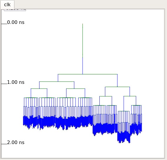
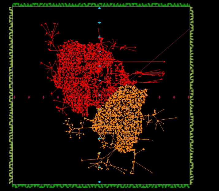
Figure 6: Clock Tree Synthesis (CTS) profile of the 2-core GPU. Top: The hierarchical tree structure demonstrating the carefully balanced buffering. Bottom: The physical routing distribution of the clock network across the die, ensuring the 100 MHz clock arrives uniformly at all internal registers with minimal skew.
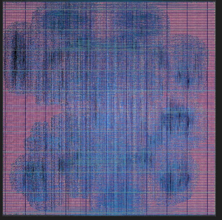
Figure 7: Final GDSII layout of the 2-core GPU architecture generated via the OpenLane EDA toolchain targeting the Skywater 130nm process node.
Results
1. Simulation vs. Real-World Silicon Performance
The disparity between software emulation and physical hardware execution highlights the immense benefits of our multi-core SIMT scaling. During early verification, a SystemVerilog stress-test testbench (tb_gpu.sv) configured with the base 2-core architecture was used to simulate the hardware executing a high-resolution 640x480 frame. To process this, the testbench dispatched exactly 307,200 threads. Simulating this immense parallel workload required approximately 4 minutes of host processing time using Verilator, accurately resolving the waveform logic to dump the computed pixels to an output_frame.hex file in 249,948 clock cycles (2.5 milliseconds of simulated hardware time).
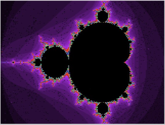
Figure 1: Simulation demonstrating the successful execution of the 640x480 Mandelbrot frame, capturing the massive thread dispatching and final memory dump.
Translating these software metrics to the physical hardware emphasizes the success of our 8-core scaling and 95 MHz timing closure. When the fully scaled system was deployed to drive the physical 800x600 VGA monitor (dispatching an even larger 480,000 threads with deep 255-iteration bounds), the Nexys 4 DDR board rendered the fractal in a fraction of a second, validating the robustness and extreme throughput of our custom silicon design.

Figure 2: The custom 8-core GPU successfully rendering the Mandelbrot set at 800x600 resolution on a physical display, colored dynamically by the hardware palette decoder. A live video demonstration of this hardware execution can be viewed here.
2. Hardware Resource Utilization & DSP Optimization
The entire SoC was synthesized, placed, and routed for the Xilinx Artix-7 FPGA (XC7A100T) present on the Nexys 4 DDR board using the Vivado Design Suite. The architecture heavily leverages the FPGA's distributed logic. Because almost the entire BRAM capacity (94.81%) was rightfully dedicated to the 800x600 asynchronous Framebuffer, the GPU's internal registers, the 8 compute cores, and the Program/Config memory domains were successfully and exclusively inferred using LUTs and Flip-Flops.
| Resource Type | Used | Available (Artix-7) | Utilization (%) |
|---|---|---|---|
| Look-Up Tables (LUTs) | 28,368 | 63,400 | 44.74% |
| Flip-Flops (FFs) | 24,611 | 126,800 | 19.41% |
| Block RAM (36E1) | 128 | 135 | 94.81% |
| DSP Slices | 129 | 240 | 53.75% |
Conclusions / Future Scope
Conclusions:
This project successfully transitioned an abstract SIMT computing logic model into a fully physical, interactive graphics-rendering silicon device. By overcoming immense routing complexity, timing violations, and dispatcher state stalling, the 8-core implementation validates the robustness and extreme throughput of our custom hardware design over sequential software emulation.
Future Scope:
- General-Purpose Hardware Division: Implement a multi-cycle stall pipeline within the ALU to support a true hardware divider without breaking clock timing.
- Advanced GPU Features: Add active/inactive thread masking to natively support branch divergence.
- Memory Optimizations: Introduce Instruction Caching and Memory Coalescing to further optimize global memory bandwidth and reduce pipeline wait states.
References & Links
- GitHub Repository: https://github.com/RushilJ2603/IEEE-Core-Cascade
- Demo Video: https://tinyurl.com/gpu-demo
- Majmudar, Adam. "Tiny-GPU: A minimal GPU design in Verilog to learn how GPUs work from the ground up." GitHub.
- Xilinx Inc. "Vivado Design Suite User Guide: Logic Simulation."
- Digilent. "Nexys 4 DDR FPGA Board Reference Manual."
Mentors and Mentees Details
Project Mentors:
- Mukul Paliwal (231EE134)
- Ratan Y Mallya (231EC146)
- Sirigiri Tarun (231EC156)
Team Members (Mentees):
- Rushil Jain (241EC148)
- Shamit Hoysal (241EE253)
- Vamshikrishna V Bidari (241EC58)
- Vikram Singh (241EC164)
Report Information
Team Members
Team Members
Report Details
Created: April 7, 2026, 6:19 p.m.
Approved by: Mayank Singh [Diode]
Approval date: None
Report Details
Created: April 7, 2026, 6:19 p.m.
Approved by: Mayank Singh [Diode]
Approval date: None