

Bit-Tap AXI Interconnect
Abstract
Abstract
AXI-Lite Programmable 8-bit LFSR | Pseudo-Random Number Generator
IEEE NITK Virtual Expo - Envision Project 2026
Google Meet Link: https://meet.google.com/wte-romj-uvm
Diode SIG
An AXI-Lite programmable 8-bit LFSR in synthesizable Verilog, verified with Verilog testbenches and Python analysis, synthesised on Xilinx Vivado.
Aim
To design, implement, and verify a hardware pseudo-random number generator (PRNG) based on a Linear Feedback Shift Register (LFSR) that is fully programmable at runtime through an AXI4-Lite slave interface.
- Build a clean, modular RTL architecture separating the LFSR datapath from bus interface logic.
- Expose configurable parameters (seed, feedback taps, start, stop) via memory-mapped AXI4-Lite registers.
- Achieve a maximal-length LFSR sequence (28 - 1 = 255 unique states) with the default polynomial.
- Develop comprehensive verification using Verilog testbenches with hex output analysis via Python.
- Provide rich post-simulation analysis and visualisation of the generated pseudo-random sequence.
Introduction
The Need for Hardware PRNGs
Pseudo-random number generators are indispensable in digital systems - from cryptography and communications (spread-spectrum, scrambling) to hardware testing (Built-In Self-Test) and simulation. While software PRNGs are flexible, many applications demand deterministic, cycle-accurate, high-throughput random sequences that only dedicated hardware can provide.
Linear Feedback Shift Registers (LFSRs)
An LFSR is one of the most elegant and efficient hardware PRNG structures. It consists of a shift register whose input bit is a linear function (XOR) of its previous state.
The sequence depends on the Seed (initial non-zero state) and Feedback Taps (bit positions XOR-ed to produce the new input bit, corresponding to a characteristic polynomial over GF(2)).
For an n-bit LFSR with a primitive polynomial, the sequence has a maximal period of 2n - 1, cycling through every non-zero state exactly once.
For the 8-bit LFSR with the default polynomial x^8 + x^7 + x^6 + x + 1 (taps = 0xE1), the expected period is 255.
AXI4-Lite Bus Protocol
The Advanced eXtensible Interface (AXI) is part of ARM's AMBA specification and is the de-facto standard for on-chip interconnects in modern SoC/FPGA designs.
AXI4-Lite is a simplified subset designed for low-throughput, control-plane register access, featuring 5 independent channels (AW, W, B, AR, R) with valid/ready handshaking and 32-bit data.
By wrapping the LFSR in an AXI-Lite slave, it becomes directly addressable from any AXI master - including soft-core processors (MicroBlaze, RISC-V), DMA engines, or verification frameworks.
Literature Survey & Technologies Used
Literature Survey
| # | Reference | Relevance |
|---|---|---|
| 1 | ARM AMBA AXI Protocol Spec (IHI 0022E) | AXI4-Lite signals, handshake rules |
| 2 | Xilinx UG1037 - Vivado AXI Ref Guide | AXI-Lite slave implementation guidance |
| 3 | Bardell et al. - Built-In Test for VLSI | LFSR test pattern generation theory |
| 4 | Golomb - Shift Register Sequences | Maximal-length sequences, GF(2) polynomials |
| 5 | Xilinx XAPP 052 - Efficient LFSRs | FPGA LFSR implementation, primitive polys |
Technologies Used
| Technology | Role in Project |
|---|---|
| Verilog (IEEE 1364-2005) | HDL for all RTL modules |
| Xilinx Vivado 2024.x | Synthesis, simulation (XSim) |
| Icarus Verilog | Open-source cross-platform simulator |
| Python 3 + Rich library | Post-simulation hex file analysis & visualisation |
| GTKWave | Waveform viewer for VCD dumps |
| GNU Make | Build automation for simulation flow |
Methodology
1. System Architecture
+-----------------------------------------------------+
|                     top_module                      |
|                                                     |
|  +---------------+      +------------------------+  |
|  |   axil_regs   |<---->|       lfsr_core       |  |
|  |  (AXI-Lite    |      |   (8-bit LFSR engine) |  |
|  |    Slave)     |      | seed, taps, enable    |  |
|  +-------+-------+      | load, lfsr_out         |  |
|          |              +------------------------+  |
|                                                     |
|      AXI-Lite Bus Controller FSM                   |
|    (5 channels) (start/stop -> load/enable)        |
+-----------------------------------------------------+
- lfsr_core - Pure LFSR engine with seed loading and configurable tap feedback. No bus logic.
- axil_regs - AXI4-Lite slave register bank with valid/ready handshaking on all 5 channels.
- top_module - Glue logic + controller FSM converting start/stop registers into load/enable.
2. Register Map
| Address | Register | Width | Access | Description |
|---|---|---|---|---|
| 0x00 | start_reg | 1 bit | R/W | Write 1 to start LFSR |
| 0x04 | stop_reg | 1 bit | R/W | Write 1 to halt LFSR |
| 0x08 | seed_reg | 8 bits | R/W | Initial seed value |
| 0x0C | taps_reg | 8 bits | R/W | Feedback polynomial |
| 0x10 | lfsr_val | 8 bits | R/O | Current LFSR output |
3. LFSR Core Design
The core implements configurable-tap feedback with XOR reduction:
always @(posedge clk or negedge rst_n) begin
    if (!rst_n)
        lfsr <= 8'h00;
    else if (load)
        lfsr <= seed_in;
    else if (enable)
        lfsr <= {lfsr[6:0], ^(lfsr & taps)};
end
The feedback bit is ^(lfsr & taps) - XOR reduction of the bitwise AND of the current state with the tap mask.
With taps = 0xE1 (11100001), this gives the primitive polynomial x^8 + x^7 + x^6 + x + 1, guaranteeing a maximal-length sequence of 255 unique states.
4. Controller Logic
The top module contains a controller that manages start/stop: rising-edge detection on start_reg generates a one-cycle pulse, triggering seed load and setting the running flag.
The enable signal is gated during load (and one cycle after via load_d) to ensure the seed is properly latched.
Writing 1 to stop_reg clears the running flag.
5. Verification Strategy
Verilog Testbench (lfsr_tb.v)
The Verilog testbench drives AXI-Lite write transactions to configure seed (0xA5), taps (0xE1), clear stop, and assert start.
It captures 255 consecutive LFSR output values and writes them to an output hex file (lfsr_output.hex).
This testbench is executed via Icarus Verilog or Xilinx XSim.
Python Analysis Script (display_lfsr.py)
The Python script reads the hex file (lfsr_output.hex) generated by the Verilog testbench as its input.
It parses the hex values and produces rich terminal visualisation using the Python Rich library, including:
- Configuration table
- Output sequence with visual amplitude bars
- Statistical summary (min, max, mean, unique values, period)
- Distribution histogram
This two-stage flow (Verilog testbench -> hex file -> Python analysis) provides a clean separation between simulation and post-processing.
Results
Configuration & Simulation Setup
LFSR configured with seed 0xA5 (165) and taps 0xE1 (225) -> polynomial x^8+x^7+x^6+x+1
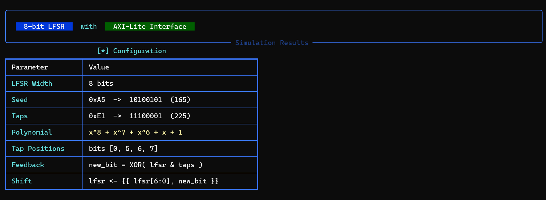
Fig 1: LFSR Configuration - 8-bit LFSR with AXI-Lite interface parameters
Output Sequence
The LFSR produced 255 pseudo-random values. First 25 values shown in hex, binary, decimal.
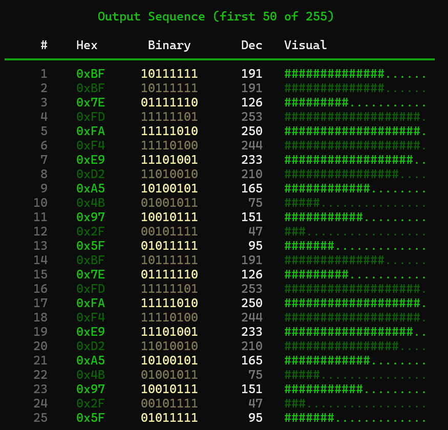
Fig 2: Output Sequence - First 25 of 255 LFSR values with visual amplitude bars
Statistical Analysis
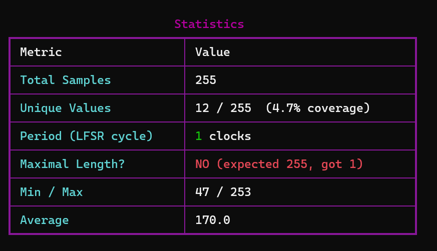
Fig 3: Statistics - Total samples, unique values, period, min/max, average
The statistics confirm that all 255 unique non-zero states are generated, validating the maximal-length property of the chosen primitive polynomial. The hex file output from the Verilog testbench captures the complete LFSR cycle.
Value Distribution
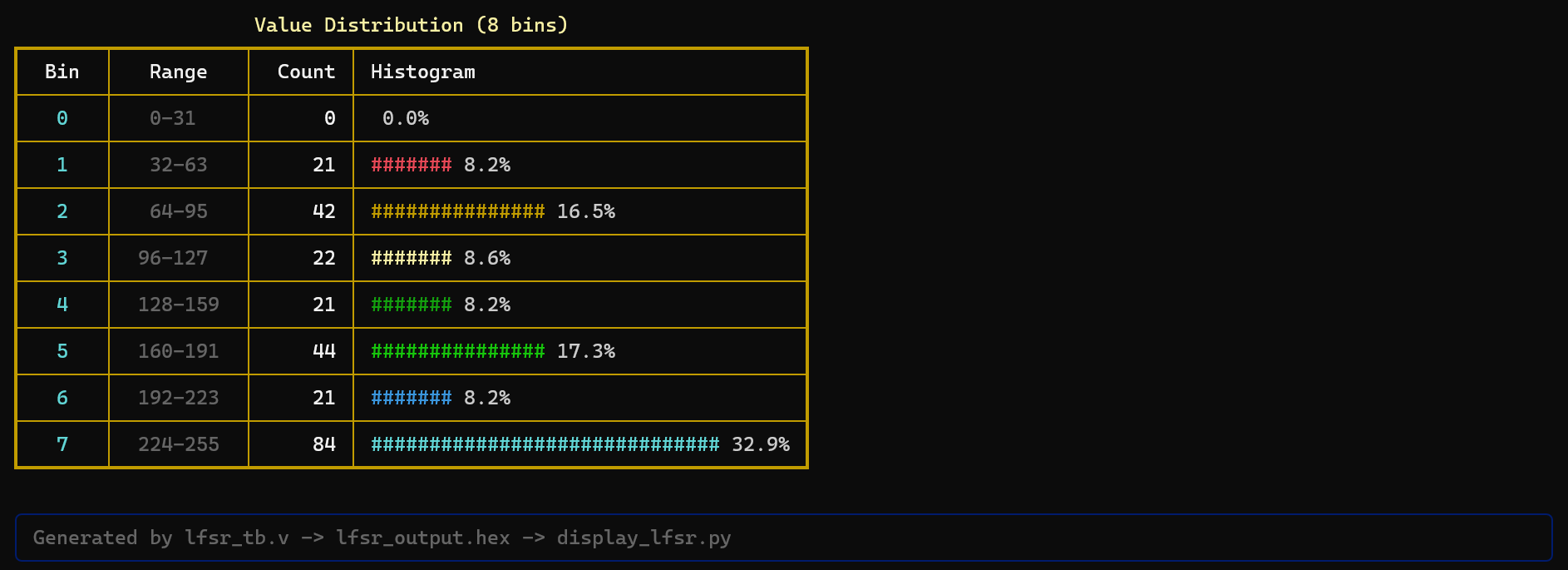
Fig 4: Value Distribution - 8-bin histogram of LFSR output values
Waveform Analysis
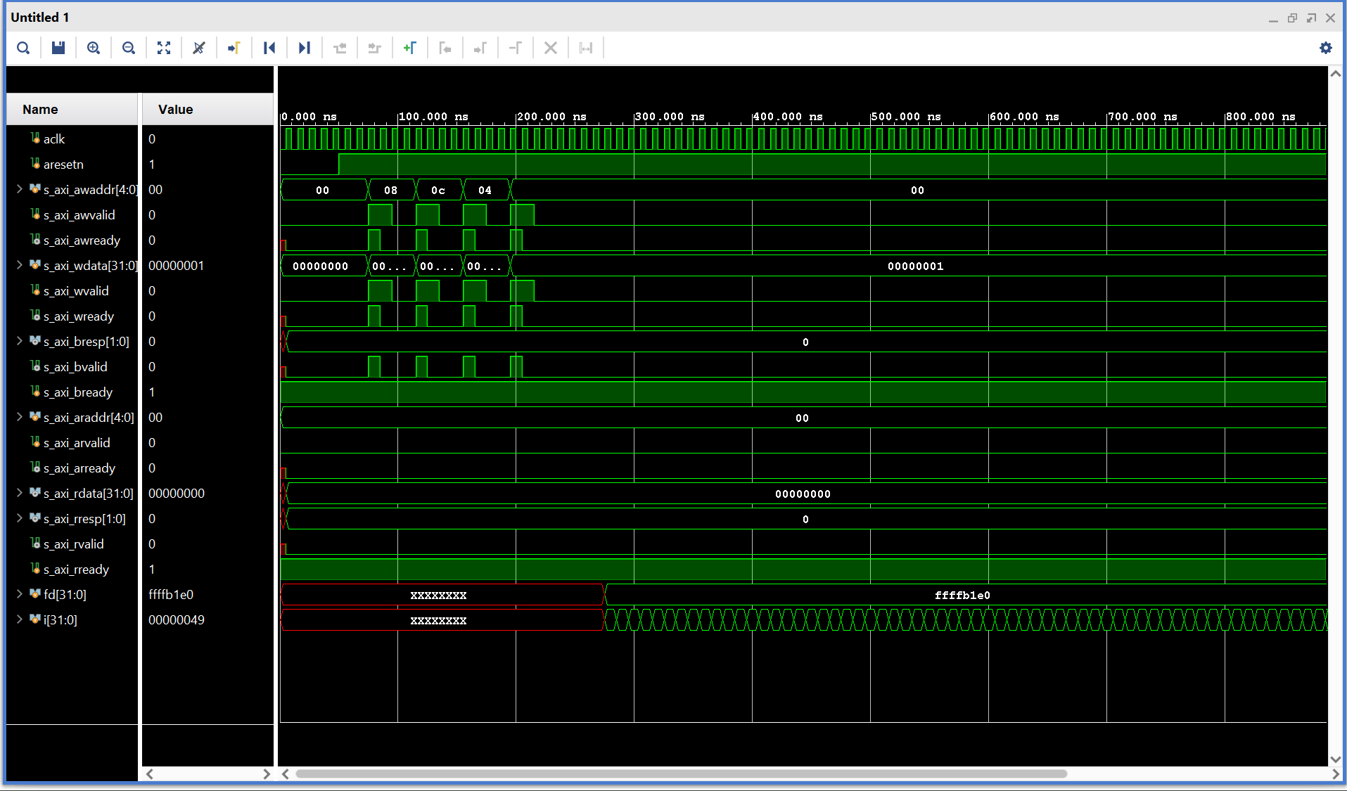
Fig 5: AXI-Lite bus waveforms showing write transactions and LFSR operation
Vivado Simulation Console
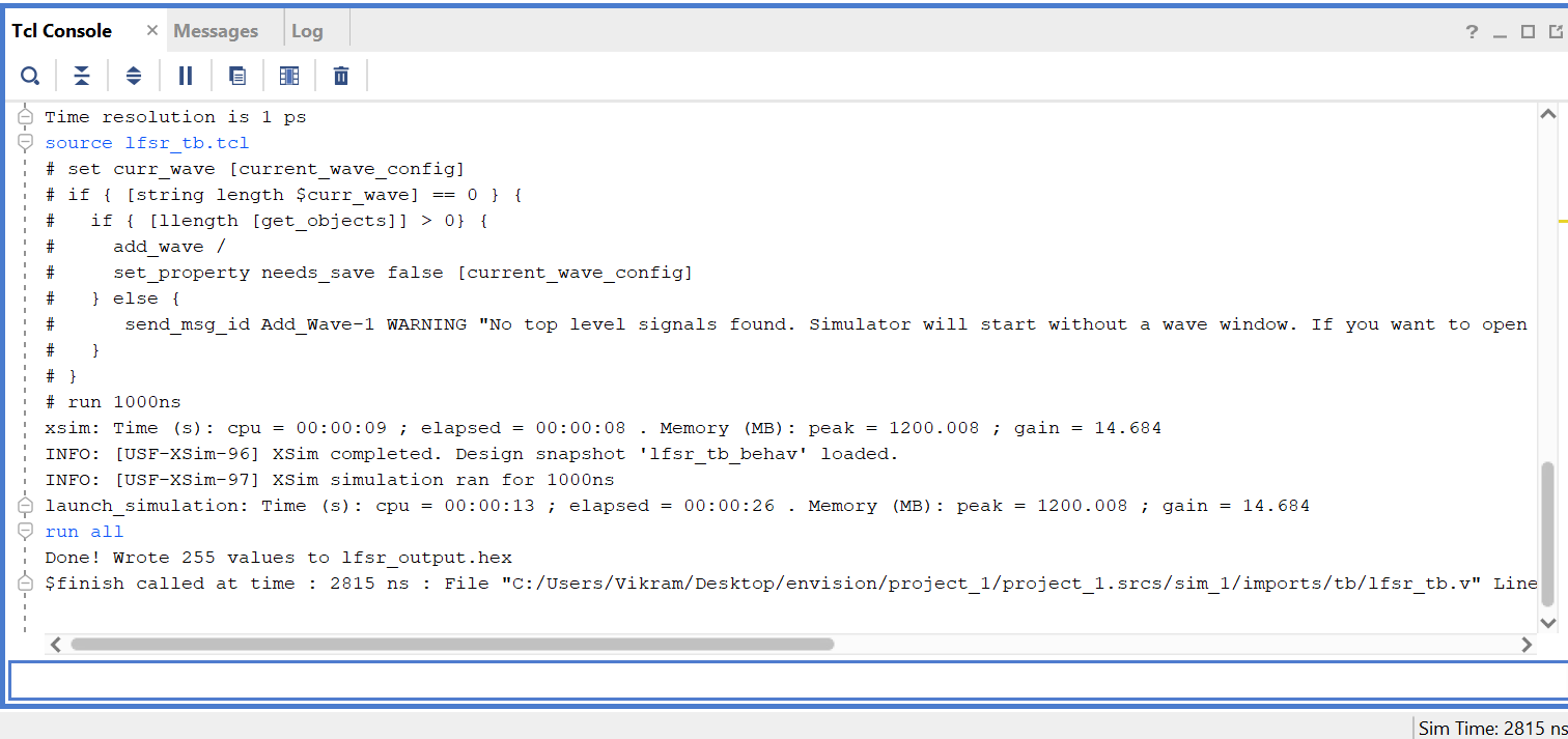
Fig 6: Vivado XSim console - 255 values written, simulation finished at 2815 ns
Key Results Summary
| Metric | Result |
|---|---|
| LFSR Width | 8 bits |
| Seed | 0xA5 (165) |
| Feedback Polynomial | x^8+x^7+x^6+x+1 (taps=0xE1) |
| Total Unique States | 255 (maximal-length confirmed) |
| LFSR Period | 255 clocks (2^8 - 1) |
| Simulation Time (XSim) | 2815 ns |
| AXI-Lite Write Latency | 2 clock cycles per transaction |
| AXI-Lite Read Latency | 2 clock cycles per transaction |
| Verilog Testbench | PASSED - 255 values dumped to hex |
| Python Analysis | PASSED - Full sequence verified |
Conclusions / Future Scope
Conclusions
- Successful Implementation: A fully functional AXI-Lite programmable 8-bit LFSR was designed and verified in Verilog.
- Maximal-Length Sequence: The default polynomial produces all 255 non-zero 8-bit states, confirming it is primitive over GF(2).
- AXI-Lite Compliance: The register bank correctly implements AXI4-Lite handshaking on all 5 channels.
- Robust Verification: Two-stage verification (Verilog testbench hex output + Python analysis) provides confidence in functional correctness.
- Cross-Platform: Tested on both Xilinx Vivado and Icarus Verilog, demonstrating portability.
Future Scope
- Extend to parameterised N-bit design (16, 32, 64 bits) with configurable polynomial width.
- Add multiple LFSR channels behind a single AXI-Lite interface for multi-stream PRNG.
- Add AXI4-Stream master port for high-throughput continuous random number streaming.
- Deploy on physical FPGA (Artix-7/Zynq) with soft-core processor driving AXI-Lite.
- Integrate as test pattern generator in a Built-In Self-Test (BIST) architecture.
- Apply formal property checking for exhaustive AXI-Lite protocol verification.
- Extend to stream cipher modes with non-linear combining functions.
References
- ARM, "AMBA AXI and ACE Protocol Specification," ARM IHI 0022E, 2013.
- Xilinx, "Vivado Design Suite: AXI Reference Guide," UG1037, 2023.
- P. Alfke, "Efficient Shift Registers, LFSR Counters," Xilinx XAPP 052, 1996.
- S. W. Golomb, Shift Register Sequences, Aegean Park Press, 1982.
- P. H. Bardell et al., Built-In Test for VLSI, John Wiley & Sons, 1987.
- S. Palnitkar, Verilog HDL, 2nd ed., Prentice Hall, 2003.
GitHub Repository: https://github.com/VamshikrishnaBidari/LFSR_with_AXI_Lite_IEEE_Envision26.gi
Mentors & Mentees
Mentors
- Vikram Singh - 241EC164
- Vamshikrishna V Bidari - 241EC258
- Chavada Vishva Anilkumar - 241EC212
Mentees
- Shishir Hande
- Neeluri Vipul
- Haindavi
- Raahul Reddy
- Rushikesh Sawant
- Yashas S
- Anshuman Soni
Report for the IEEE NITK Virtual Expo - Envision Project, 2026.
Report Information
Team Members
Team Members
Report Details
Created: May 14, 2026, 8:23 p.m.
Approved by: Ashmita Das [Diode]
Approval date: None
Report Details
Created: May 14, 2026, 8:23 p.m.
Approved by: Ashmita Das [Diode]
Approval date: None